UV Optoelectronic Devices based on A1GaN Alloys
3 Forbes Road
Lexington, MA 02421
USA
Photonics Society – 6:30PM, Thursday, 8 October
UV Optoelectronic Devices based on AlGaN alloys
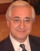
Theodore D. Moustakas – Electrical and Computer Engineering – Photonics Center, Boston University
The GaN-AlN material system is well suited for UV optoelectronic devices (LEDs, lasers, electroabsorption modulators etc.) because its energy gap can be tuned by changing its alloy composition to cover all three regions of the UV electromagnetic spectrum {UV-A (340-400 nm), UV-B (290-340 nm) and UV-C (200-290 nm). Such semiconductor devices are expected to be lightweight, compact and have low power requirements. In addition nitride semiconductors are physically robust, chemically inert, have high corrosion resistance and are non-toxic. These properties make them also attractive for use in hostile environments and at high temperatures.
In this talk I will discuss the development of AlGaN films with strong band structure potential fluctuations, which led to deep UV emitting Al0.7Ga0.3N/AlN multiple quantum wells with internal quantum efficiency (IQE) as high as 70%, and maximum net modal gain in excess of 100 cm-1 under femtosecond optical pumping at relatively low transparency threshold of about 1017 cm-3 excited carriers. The employment of these materials for the development of deep UV LEDs, lasers, and electroabsorption modulators will be discussed.
Biography
Dr. Moustakas is the inaugural Distinguished Professor of Photonics and Optoelectronics at Boston University. He received his PhD from Columbia University in 1974. He held research positions at Harvard University and Exxon Corporate Research Laboratory prior to joining Boston University in 1987 as a Professor of Electrical and Computer Engineering. He is also a Professor of Physics and Associate Head of the Division of Materials Science and Engineering.
Dr. Moustakas is a Fellow of the American Physical Society (1994), the Electrochemical Society (1997), a Charter Fellow of the National Academy of Inventors (2012), and the Institute of Electrical and Electronic Engineers-IEEE (2014). He holds an honorary doctoral degree from the Aristotle University (2003); he received the MBE Innovator Award in 2010; in 2011 he received the Distinguished Scholar Award from the BU College of Engineering and in 2013 he received the Boston University Innovator of the Year Award. Intellectual property that resulted from his work has been licensed to a number of companies, including major manufacturers and users of blue LEDs and lasers (Cree, Nichia, Philips, OSRAM, Apple, Google, Amazon, Samsung, LG, Sony etc.).
This meeting begins at 6:30 PM Thursday, October 8th, 2015 and will be located 3 Forbes Road (an MIT Lincoln Laboratory facility), Lexington, MA, 02420. The meeting is free and open to the public. All are welcome. Prior to the seminar there will be social time and networking from 6:30 – 7:00PM. Dinner will also be provided. The seminar will begin at 7:00PM. For more information contact Jade Wang, Boston IEEE Photonics Society Chapter chair at jpwang@ll.mit.edu, or visit the Boston IEEE Photonics Society website at www.bostonphotonics.org.
Directions to Forbes Rd Lincoln Laboratory: (from interstate I-95/Route 128)
Take Exit 30B onto Marrett Rd in Lexington – Merge into left lane
Make the first Left onto Forbes Rd.
Proceed straight through the small rotary and enter the parking lot.
The entrance is on your right.
To assist us better plan this meeting, please pre-register at: http://www.ieeeboston.org/Register/

