III-V Lasers Grown on (001) Si Emitting at Communication Wavelengths
3 Forbes Rd
Lexington, MA 02421
USA
Photonics Society
To support an energy-efficient optical interconnect technology enabled by silicon photonics, development of low-power-consumption active devices and associated integration technologies is needed. Quantum dot (QD) active layers grown on lattice-matched III-V substrates have demonstrated their benefits for lasers with low-thresholds and temperature-independent operation. In addition, the reduced sensitivity of QD to defects and their unique capability of filtering dislocations make them an ideal candidate as the gain medium of hetero-integrated III-V on Si optical sources. In this talk, I will discuss the growth of multi-stack InAs QDs on compliant III-V/Si substrates by MOCVD. Fabrication and laser characteristics of whispering-gallery-mode (WGM) micro-lasers using the grown epitaxial structures will also be discussed. The micro-disk lasers were one to four microns in diameter, with single mode lasing at either 1.3 or 1.55 µm, depending on the barrier/cladding system. With smooth sidewalls and sufficient undercut by wet etching of the pedestal, the air-cladded MDs exhibit ultra-low thresholds of a few W by optical pumping. Results of electrically-pumped micro-lasers will also be presented. Using the aspect ratio trapping (ART) method, we grew high crystalline quality, well-aligned, in-plane InP/InGaAs nano-ridges on nominal (001) Si substrates. We demonstrate for the first time room-temperature (RT) lasing at telecom-bands from InP/InGaAs nano-ridges. The InGaAs quantum wells (QWs) emitting at telecom-wavelengths were grown inside InP nano-ridges on patterned (001) Si. Then, we achieve lasing through optical pumping after transfer of the InP/InGaAs nano-ridges onto SiO2/Si substrates.
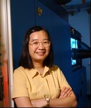
Prof. Kei May Lau, Fang Professor of Engineering, Hong Kong University of Science and Technology, Kowloon, Hong Kong
Kei May Lau is Fang Professor of Engineering at the Hong Kong University of Science and Technology (HKUST). She received the B.S. and M.S. degrees in physics from the University of Minnesota, Minneapolis, and the Ph.D. degree in Electrical Engineering from Rice University, Houston, Texas. She was on the ECE faculty at the University of Massachusetts/Amherst and initiated MOCVD, compound semiconductor materials and devices programs. Since the fall of 2000, she has been with the ECE Department at HKUST. She established the Photonics Technology Center for R&D effort in III-V materials, optoelectronic, high power, and high-speed devices. Professor Lau is a Fellow of the IEEE (2001), a recipient of the US National Science Foundation (NSF) Faculty Awards for Women (FAW) Scientists and Engineers (1991), Croucher Senior Research Fellowship (2008), and the IEEE Photonics Society Aron Kressel Award (2017). She is an Editor of the IEEE EDL and Associate Editor of Applied Physics Letters.
This meeting begins at 7 PM Wednesday, May 30th, 2018 and will be located at 3 Forbes Road, Lexington, MA, 02420. Note this is a satellite location ~1.5mi away from MIT Lincoln Laboratory.
The meeting is free and open to the public. All are welcome. Prior to the seminar there will be social time and networking from 6:30 – 7:00PM. Pizza will also be provided. The seminar will begin at 7:00PM.
For more information contact Ajay Garg, IEEE Boston Photonics Society chair at ajay.sinclair.garg@ieee.org, or visit the IEEE Boston Photonics Society website at www.bostonphotonics.org.
Directions to 3 Forbes Rd Lincoln Laboratory: (from interstate I-95/Route 128)
Take Exit 30B onto Marrett Rd in Lexington – Merge into left lane
Make the first Left onto Forbes Rd.
Proceed straight through the small rotary and enter the parking lot.
The entrance is by the flags.

